1. What Is a Parallel Interface?
A parallel interface transmits multiple bits simultaneously across multiple data lines. As shown below, there are 8 to 32 or more data wires (D[7:0], D[31:0], etc.) between transmitter and receiver, along with a shared clock and control signals such as VALID and READY.
┌─────────────┐         ┌─────────────┐
│ Transmitter │  D[7:0] │  Receiver   │
│             ├────────►│             │
│             │  CLK    │             │
│             ├────────►│             │
│             │  VALID  │             │
│             ├────────►│             │
└─────────────┘         └─────────────┘
Advantages:
- Simple, intuitive structure — easy to design and debug
- High bandwidth at low frequency (e.g., 8-bit × 100 MHz = 800 Mbps)
- No serializer/deserializer needed → low latency
- Shared clock makes synchronization straightforward
2. Limitations and Real-World Problems
(1) Pin Count and PCB Complexity
As data width increases, package pin count, PCB routing complexity, and cost grow rapidly.
Example: A 32-bit parallel bus requires 32 data + 1 clock + 2–4 control = 35–37 pins
(2) Skew — The Enemy of Timing
All data bits must arrive simultaneously, but in practice each trace has slightly different lengths, impedances, and loads — causing arrival time differences known as skew. At high speeds, skew becomes critical.
CLK  ──┐  ┌──┐  ┌──
       └──┘  └──┘
D[0] ───────────────  ← Ideal (no delay)
     ∆t₁↕
D[1] ───────────────  ← Delay from trace length difference
     ∆t₂↕
D[2] ───────────────  ← Additional delay
Real-world impact:
- At 1 GHz (1 ns period), 200 ps of skew consumes 20% of the timing budget
- A 1 cm trace length difference ≈ 60–70 ps of skew (propagation speed ~15–17 cm/ns)
- Excessive skew causes setup/hold violations and data errors
Solutions:
- Trace length matching (serpentine routing) is mandatory in PCB layout
- Validate skew, reflections, and jitter using SI simulation (IBIS models, etc.)
(3) EMI and Crosstalk
When multiple signals switch simultaneously, electromagnetic interference (crosstalk) and SSN (Simultaneous Switching Noise) appear between adjacent lines — making FCC/CE EMC certification significantly harder to pass.
(4) Signal Integrity at High Frequencies
As frequency increases, reflections, ringing, overshoot, and undershoot become critical SI problems.
Power consumption scales with both width and frequency:
$$P = C \times V^2 \times f \times N_{bits}$$
Increasing width worsens pin count, PCB complexity, EMI, and power. Increasing frequency worsens SI, skew, and EMI. Both directions have hard physical limits.
(5) Board and Cable Design Difficulty
- All traces must be matched to within picoseconds — PCB layout becomes extremely complex
- Longer cables accumulate more skew; connector and cable costs increase accordingly
Practical design tips:
- Route data, clock, and control traces on the same layer with matched impedance and serpentine length matching
- For high-speed parallel buses like DDR, use per-byte DQS (source-synchronous strobe) to contain skew to within each byte lane
- Apply Write Leveling and Read Training to compensate for board-specific timing variation
3. Real-World Examples and the Evolution to Serial
(1) DDR4 Memory Interface
- 64-bit data + 8-bit ECC = 72 signals total
- Each byte lane has its own DQS strobe signal → skew correction per byte group
- Write Leveling and Read Training automatically compensate for board-level timing variation
(2) PCI → PCIe Evolution
| Interface | Type | Bus | Frequency | Bandwidth |
|---|---|---|---|---|
| PCI | Parallel | 32-bit shared | 33 MHz | 133 MB/s |
| PCI-X | Parallel | 64-bit shared | 133 MHz | 1,066 MB/s |
| PCIe Gen1 x16 | Serial | 16 lanes × 1 pair | 2.5 Gbps/lane | ~4 GB/s |
| PCIe Gen5 x16 | Serial | 16 lanes × 1 pair | 32 Gbps/lane | ~64 GB/s |
The industry shifted from parallel shared buses to serial point-to-point links — drastically reducing pin count while multiplying bandwidth by orders of magnitude.
4. Verilog Example
| |
This module registers 8-bit parallel data with a 1-clock pipeline delay — the foundation of synchronous parallel data transfer in FPGA and ASIC design.
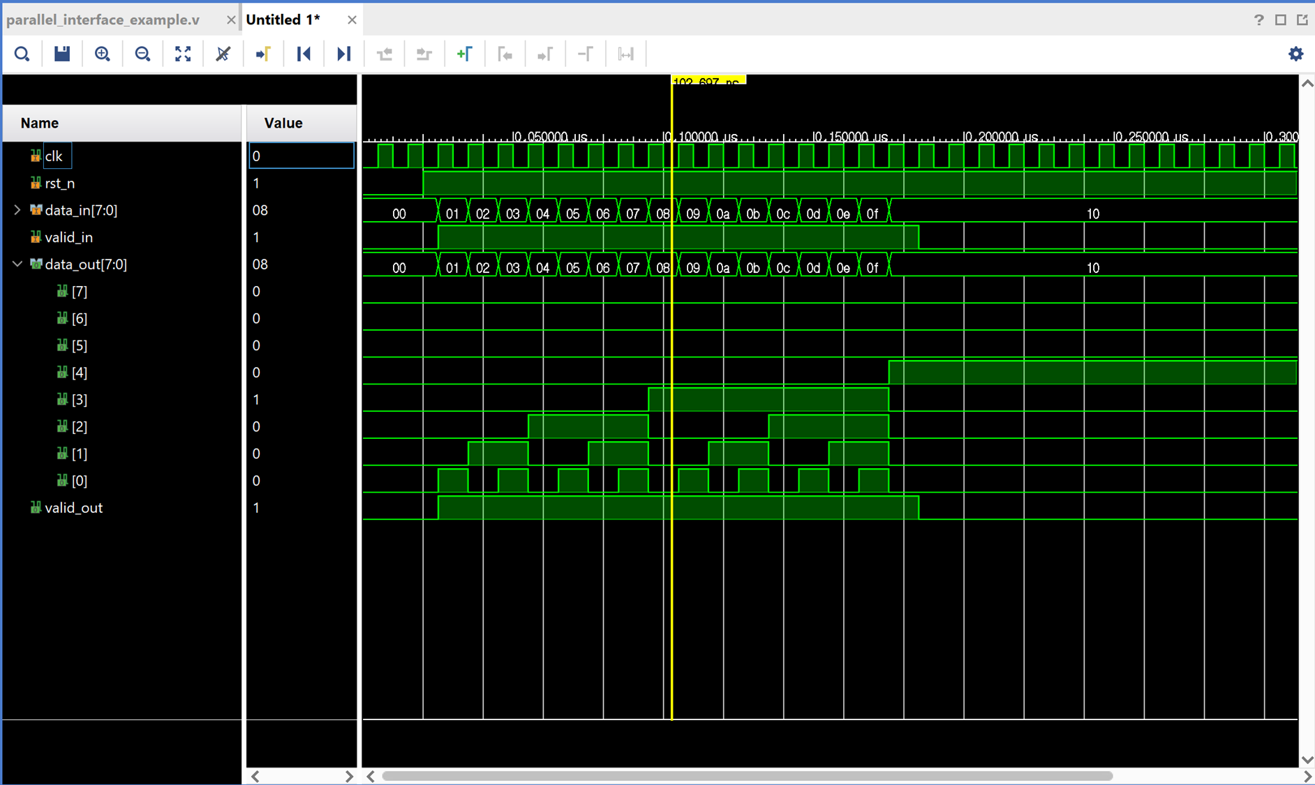
Waveform behavior: data_in is captured on the rising edge of clk, and data_out appears one clock cycle later. The valid signal is delayed identically to maintain handshake timing.
5. Summary
- Parallel interfaces are intuitive and easy to implement, but face hard physical, electrical, and economic limits at high speeds.
- Skew, EMI, signal integrity, and cost constraints collectively push high-speed designs toward source-synchronous (DQ+DQS) or fully serial (PCIe, USB, etc.) architectures.
- When designing parallel interfaces, always apply trace length matching, SI simulation, and calibration techniques such as Write Leveling and Read Training.